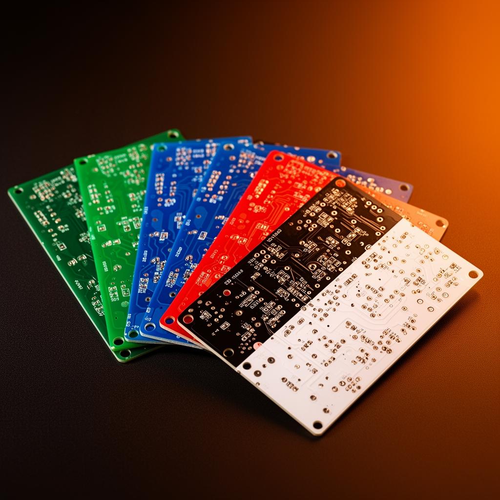
PCB Technology
Advanced constructions, mastered.
Sunrise invests in the equipment and process know-how to manufacture the technologies pushing modern electronics forward — without sacrificing the speed you expect from us.
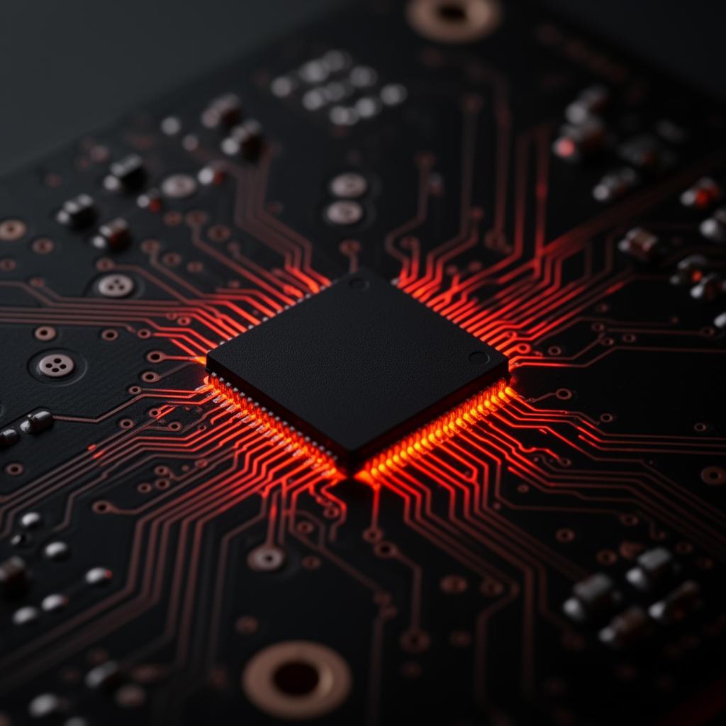
HDI & Microvia
High-density interconnect with stacked and staggered microvias for advanced miniaturization. Sequential lamination supported.
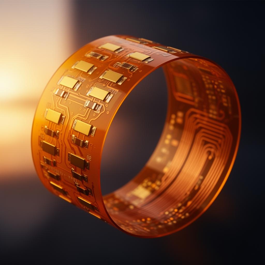
Rigid-Flex
Combined rigid and flexible sections for 3D packaging applications, eliminating connectors and reducing weight.
RF & Microwave
Rogers, Taconic and PTFE-based laminates for controlled impedance, high-frequency, and microwave applications.
Heavy Copper
Copper weights from 2 oz up to 10 oz for power electronics, motor controls and high-current designs.
Metal Core (MCPCB)
Aluminum and copper-core PCBs for thermal management in LED lighting and high-power applications.
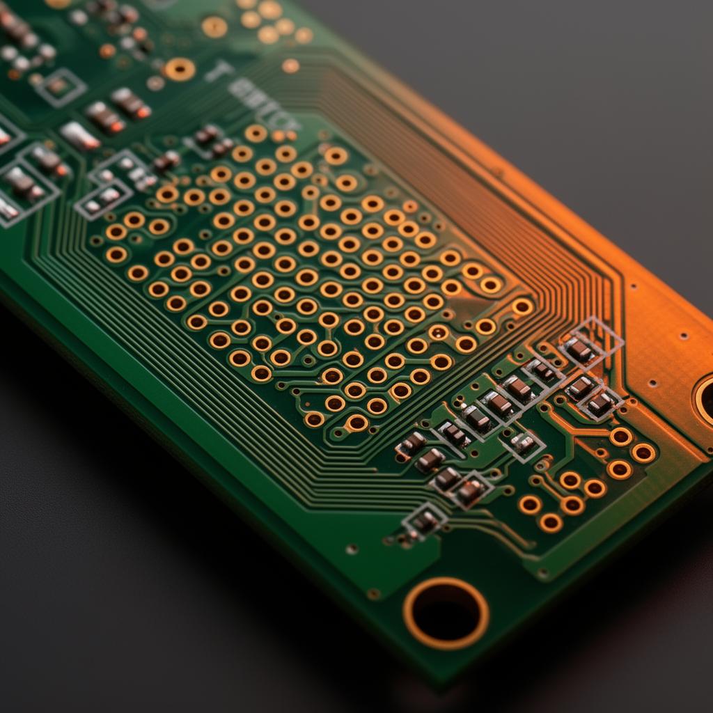
Backplane & Multilayer
Up to 44-layer multilayer constructions with sequential lamination and tight registration tolerances.
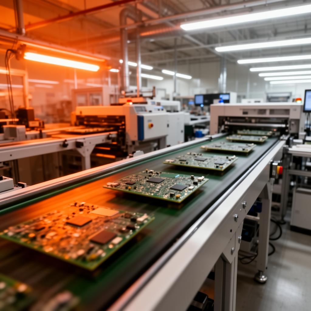
Our Process
Six steps. Zero surprises.
Design Review (DFM)
Free design-for-manufacturability review before production. We catch issues early.
Material Selection
Engineering support to pick the right laminate, copper weight, and finish for your application.
Tooling & Imaging
LDI direct imaging for fine features and precise registration on high-layer-count boards.
Drilling & Plating
Mechanical and laser drilling, with controlled-depth and back-drilling capability.
Lamination & Etch
Sequential lamination for HDI builds. Tight impedance control through fine-line etching.
Test & Inspection
100% electrical test, AOI, X-ray for BGAs, and IPC-A-600 visual inspection on every board.